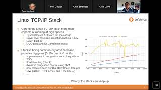
RDMA and Linux TCP - Zero-Copy Kernel Bypass for High-Performance Networking
Dive into high-performance networking with RDMA interfaces and Linux TCP stack optimization, exploring zero-copy techniques and kernel bypass for achieving 800Gbps throughput.

Universal Chiplet Interconnect Express - Building an Open Ecosystem of Chiplets
Discover how UCIe technology enables mixing chiplet components from multiple vendors for customized System-on-Chip construction, addressing growing compute demands across various sectors.
Device Security in the OCP Supply Chain - Overview of How OCP SAFE Addresses Device Firmware Challenges
Explore how OCP S.A.F.E. framework tackles device firmware security challenges and strengthens supply chain integrity through expert insights and practical solutions.
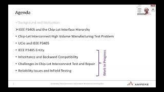
Chip-let Interconnect Test and Repair
Explore advanced techniques for testing and repairing chip-let interconnects, focusing on practical solutions and emerging methodologies in semiconductor manufacturing.

How Industry Uncertainty Impacts MEMS Commercialization - Results of the 2021 MEMS Industry Report Card Study
Explore the comprehensive analysis of MEMS industry commercialization through the 2021 Report Card study, examining COVID-19's impact and strategic recommendations for future success.
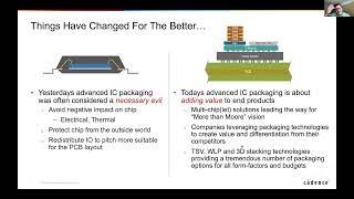
The Challenges of Scaling Beyond Moore's Law - From Monolithic Dies to 3D Heterogeneous Integration
Explore the shift beyond Moore's Law into 3D heterogeneous integration, examining technical challenges, economic factors, and emerging solutions in semiconductor design and packaging.
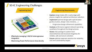
Signal Integrity Analysis for 2.5D/3D IC Technology in the Interposer Era
Delve into signal integrity analysis challenges and solutions for 2.5D/3D IC technology, focusing on silicon interposers, electromagnetic simulation, and advanced packaging architectures.
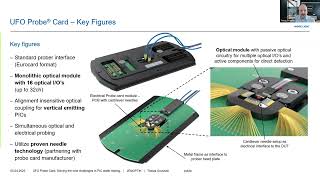
Enabling High Volume Data Communication - Solving Challenges in PIC Wafer Testing
Discover how Photonic Integrated Circuits revolutionize data communication through wafer testing innovations, focusing on Jenoptik's UFO Probe® card for simultaneous electrical and optical testing at high volumes.

Solving Moore's Law Packaging Challenges Through Next-Generation Materials and 3D Integration
Explore advanced semiconductor packaging solutions addressing Moore's Law limitations through heterogeneous integration, 3D stacking, and innovative copper interconnect materials for enhanced performance and miniaturization.
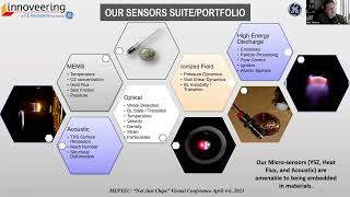
Packaging of Sensors for High Reliability, Survival and Performance in Extreme Environments
Explore sensor packaging design challenges for extreme aerospace environments, focusing on MEMS integration, material selection, and reliability testing for hypersonic applications.
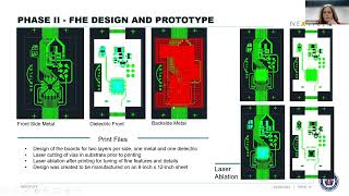
Novel Techniques for IC Integration and Packaging Using Additive Technologies
Explore innovative Flexible Hybrid Electronics manufacturing techniques combining thinned dies, printed components, and flexible materials to revolutionize electronics packaging and system integration.
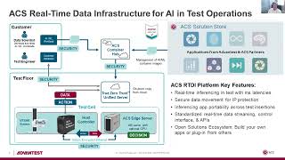
Infrastructure and Applications for AI in Semiconductor Test
Explore cutting-edge AI applications and infrastructure developments in semiconductor testing, focusing on optimization and efficiency improvements in manufacturing processes.
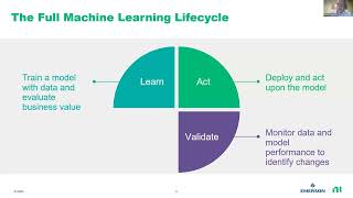
Implementing Real-time AI in High Volume Test
Discover practical strategies for implementing AI solutions in high-volume semiconductor testing environments, focusing on real-time applications and efficiency optimization.
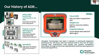
Finding the Needle in the Haystack - On the Use of AI in Defect Analysis
Explore how artificial intelligence revolutionizes semiconductor defect analysis, enhancing detection accuracy and streamlining quality control processes in manufacturing.

Big Strides in Electronics Test and Production - From Algorithmic Methods to Unsupervised Machine Learning
Discover how algorithmic methods and unsupervised machine learning are revolutionizing electronics testing and production processes for enhanced efficiency and automation.

AutoChip - Using Large Language Models to Automate IC Design
Discover how Large Language Models are revolutionizing integrated circuit design automation, enhancing efficiency and innovation in semiconductor development.
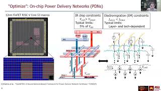
The Role of Machine Learning in Electronic Design Automation
Explore how machine learning revolutionizes electronic design automation, enhancing semiconductor development and improving design efficiency through AI-driven solutions.
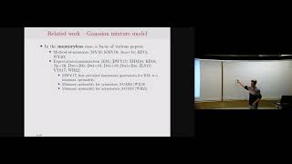
Mean Estimation in High-Dimensional Binary Markov Gaussian Mixture Models
Delve into high-dimensional mean estimation in binary Markov Gaussian mixture models, exploring how memory in data affects estimation error and the interplay between sample size, dimension, and signal strength.
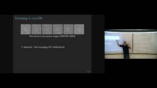
Manifold Denoising with Application to Electron Microscopy
Discover advanced manifold denoising techniques for electron microscopy image processing, focusing on Fourier-like basis construction and filtering methods to enhance two-dimensional image collections through mathematical analysis.

Real-World AI: Risk and Robustness in Reinforcement Learning and Kalman Filtering
Explore real-world applications of AI through risk-aware reinforcement learning and robust Kalman filtering, focusing on practical challenges and solutions for handling uncertainties in AI systems.
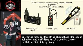
Revealing Microphone Nonlinear Behavior and Building an Ultrasonic Jammer
Discover how to exploit microphone nonlinearity and build ultrasonic jammers for enhanced privacy protection, exploring advanced counter-surveillance techniques and practical implementations.