How to Decide on Your PCB Layer Ordering, Pouring and Stackup - With Rick Hartley
Expert insights on PCB layer ordering, pouring, and stackup for optimal design. Learn techniques to minimize EMI problems and improve signal integrity in multi-layer boards.
Understanding Crosstalk in PCB Layout - You May Wish You Knew This Before
Comprehensive exploration of PCB crosstalk, covering microstrip analysis, impedance effects, and measurement techniques. Practical insights for engineers to optimize PCB layouts and minimize signal interference.

Ground in PCB Layout - Separate or Not Separate?
Explore PCB grounding techniques with expert Rick Hartley, discussing the pros and cons of separating digital and analog grounds, and best practices for effective PCB layout and signal integrity.

Is KiCad Ready to Replace Paid PCB Design Software?
Explore KiCad's capabilities, future, and potential as a free PCB design tool with project leader Wayne Stambaugh in this comprehensive interview discussing features, support, and industry adoption.
Thinking to Simulate Your PCB Layout? This May Help - With Steve Sandler
Explore PCB layout simulation techniques to uncover unexpected behaviors, analyze power plane resonances, and optimize signal integrity for improved design outcomes.

What Book for PCB Layout - Answering This and Other Questions
Expert advice on becoming a great hardware engineer, covering education, skill development, and recommended resources for PCB design and electronics.
PCB Stackups - Use Them
Explore various PCB stackup designs for different applications, from high-density to cost-effective options. Learn about motherboard, system-on-module, and SODIMM layouts to enhance your PCB design skills.
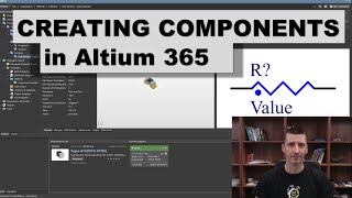
How to Create & Use Components in Altium 365 and Concord PRO
Comprehensive guide to creating and managing components in Altium 365 and Concord PRO, covering symbol creation, footprints, templates, lifecycle management, and practical applications.
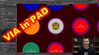
Using VIA in PAD - Guidelines, Dimensions and More
Comprehensive guide on VIA and VIA-in-PAD usage in PCB design, covering dimensions, types, limitations, and best practices for optimal board performance.
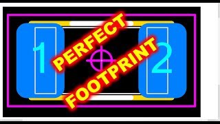
How to Create Perfect PCB Footprint - What You Really Need to Know
Learn essential PCB footprint design techniques, including pad dimensions, pin placement, and IPC standards. Gain insights into optimal practices for creating reliable and efficient PCB layouts.
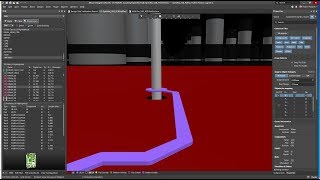
Understanding PCB Layout Essentials - Change the Way How You Look at the Tracks
Explore a new perspective on PCB layout, focusing on energy transfer rather than voltages and currents. Learn to optimize designs for improved performance and efficiency.
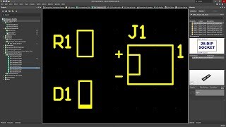
Generating Manufacturing Outputs for Altium Beginners
Learn to generate essential manufacturing outputs in Altium Designer, including Gerbers, BOMs, assembly drawings, and 3D models. Master the final steps of PCB design for production.
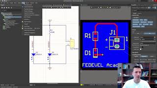
Altium Beginners - Placement, Variants, Assembly Drawings
Learn advanced Altium Designer techniques for PCB layout, including component placement, assembly drawings, and variant creation. Enhance your skills in efficient PCB design workflows.

Altium Beginners - PCB Layout
Step-by-step guide to PCB layout in Altium Designer, covering importing schematics, component placement, layer management, and design rule checks for beginners.
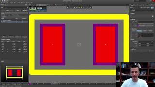
How to Create Footprints for Altium Beginners
Comprehensive guide on creating PCB footprints in Altium Designer, covering resistors, LEDs, connectors, 3D models, and schematic symbol integration for beginners.

Altium Beginners: How to Draw Schematic and Create Schematic Symbols
Step-by-step guide for beginners to create schematic symbols and draw schematics in Altium Designer, covering project setup, symbol creation, and schematic drawing techniques.
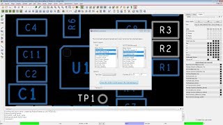
Cadence Allegro Tutorial - How to Create SKILL Script and Your Own Commands
Learn to create and use SKILL scripts for custom commands in Cadence Allegro. Covers script creation, execution, and practical application with downloadable example code.
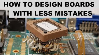
How to Design Boards That Work the First Time
Learn effective PCB design techniques to create successful first-version boards. Covers schematic design, component selection, layout strategies, and testing considerations for reliable prototypes.
Create a Wi-Fi Extender with a $3 ESP8266
Extend Wi-Fi range using a $3 ESP8266 microcontroller. Learn to modify Arduino examples for custom access points and explore two network extension methods.
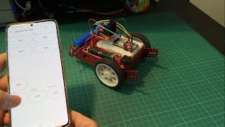
Remote Control ESP32-S IoT Car with Blynk IoT - Cloud Tutorial
Build and control an ESP32-S IoT car using Blynk cloud. Learn hardware assembly, wiring, Blynk setup, and Arduino programming for remote operation via smartphone app.
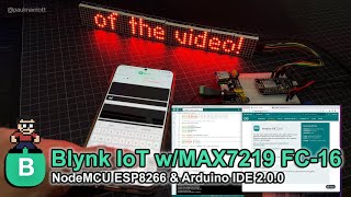
MAX7219 FC-16 64x8 Dot Matrix Display System with Blynk IoT, NodeMCU ESP8266 and Parola - Tutorial
Learn to build and program a 64x8 dot matrix display system using NodeMCU ESP8266, integrating it with Blynk IoT for remote control and monitoring via smartphone and web dashboard.