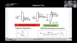
ABACUS Tool Suite and MOS Capacitors - Fall 2023
Explore MOS capacitors using ABACUS tool suite. Experiment with doping, structural parameters, and advanced effects in this hands-on semiconductor education session.
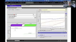
ABACUS Tool Suite and PN Junctions - Fall 2023
Explore PN junctions using ABACUS tool suite. Learn about band edge diagrams, charge distributions, and doping effects through interactive simulations powered by industrial-grade technology.
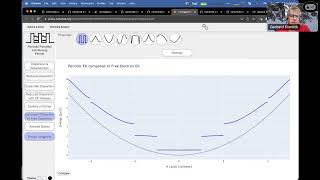
ABACUS Tool Suite: Bandstructure and Band Models - Fall 2023
Explore bandstructure tools in ABACUS, including Kronig-Penney model and sophisticated Tight Binding models. Gain insights into band formation, effective masses, and strain effects in bulk materials and nanowires.
Tuning Correlations, Topology, and Magnetism in Semiconductor Moiré Materials
Explore semiconductor moiré materials and their impact on correlations, topology, and magnetism with Stanford researcher Ben Feldman in this advanced physics lecture.
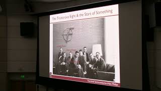
In Search for the Next Magic Stone - Applied Physics and Physics Colloquium
Explore the impact of materials on human civilization, from silicon's role in the information age to the search for new quantum matter using modern spectroscopy tools.
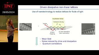
Quantum Fluids of Light in Semiconductor Lattices
Explore quantum fluids of light in semiconductor lattices, focusing on photonic resonators, polariton condensates, and topological properties. Gain insights into driven dissipative physics and its applications.
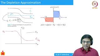
Energy Band Diagram of PN Junction
Explore the energy band diagram of PN junctions, understanding their structure and behavior in semiconductor devices.
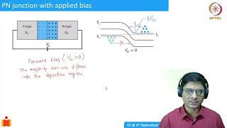
Forward and Reverse Biased PN Junctions - Lecture 5.1
Explore forward and reverse biased PN junctions, understanding their behavior and applications in semiconductor devices.
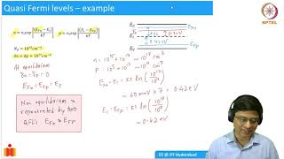
Quasi Fermi Level in Nonequilibrium Conditions
Explore quasi Fermi levels in nonequilibrium conditions, understanding their significance and applications in semiconductor physics and device analysis.
PN Junctions - An Introduction
Explore PN junctions, their formation, and fundamental principles in semiconductor physics. Gain insights into this crucial electronic component's behavior and applications.
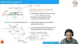
An Ideal MOS Capacitor - Lecture 6.4
Explore the characteristics and behavior of ideal MOS capacitors, understanding their fundamental principles and applications in semiconductor devices.
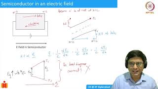
Semiconductor Bands in an Electric Field - Lecture 3.1
Explore semiconductor band behavior under electric fields, examining key concepts and implications for electronic device performance.
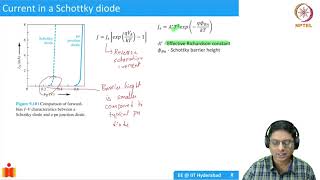
Current Flow Across a Schottky Barrier - Lecture 6.2
Explore current flow mechanisms across Schottky barriers, understanding key concepts and applications in semiconductor devices.
MOSCAP Capacitance-Voltage (CV) Characteristics - Lecture 8.2
Explore MOSCAP capacitance-voltage characteristics, analyzing their behavior and implications for semiconductor device performance and design.
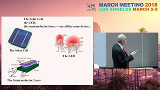
The Double-Heterostructure Concept in Lasers, LED's, and Solar Cells
Explore double-heterostructure concept in lasers, LEDs, and solar cells. Learn about semiconductor physics, electronic confinement, and device optimization from a renowned expert.
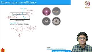
Operation of a Light Emitting Diode (LED) - Lecture 12.3
Explore the functionality and principles behind light emitting diodes (LEDs), understanding their operation and applications in modern electronics.
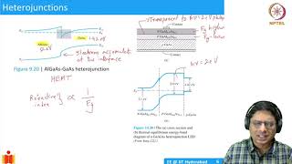
LED Emission Spectrum - Lecture 12.4
Explore the emission spectrum of LEDs, understanding their light output characteristics and applications in various fields.
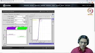
Demo of PN Junction Lab on Nanohub - Lecture 4.6
Explore PN junction behavior using Nanohub's interactive lab simulation. Gain hands-on experience with semiconductor physics concepts.
Temperature Dependence of Fermi Level
Explore the temperature-dependent behavior of the Fermi level in semiconductors, understanding its impact on electronic properties and device performance.
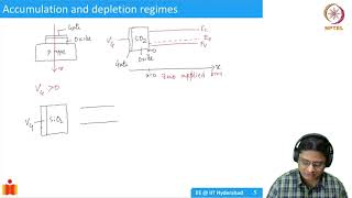
Simplified Band Diagrams of Accumulation and Depletion in MOSCAP - Lecture 6.6
Explore simplified band diagrams for accumulation and depletion in MOSCAP, enhancing understanding of semiconductor device physics and electronic behavior in metal-oxide-semiconductor structures.
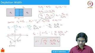
Depletion Width and Peak Electric Field in Semiconductor Devices - Lecture 4.4
Explore depletion width and peak electric field concepts in semiconductor physics, enhancing understanding of pn junction behavior and device characteristics.