Semiconductor Physics Class 12
You will learn about energy bands, valence and conduction bands, intrinsic and extrinsic properties, semiconductors, diodes, solar cells, transistors, digital and analog signals, logic gates, and much more.
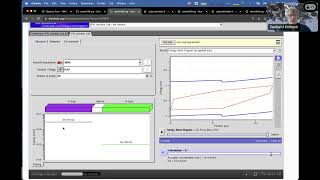
ABACUS Tool Suite and PN Junctions - Fall 2023
Explore PN junctions using ABACUS tool suite. Learn about band edge diagrams, charge distributions, and doping effects through interactive simulations powered by industrial-grade technology.
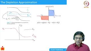
Energy Band Diagram of PN Junction
Explore the energy band diagram of PN junctions, understanding their structure and behavior in semiconductor devices.
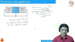
Forward and Reverse Biased PN Junctions - Lecture 5.1
Explore forward and reverse biased PN junctions, understanding their behavior and applications in semiconductor devices.
PN Junctions - An Introduction
Explore PN junctions, their formation, and fundamental principles in semiconductor physics. Gain insights into this crucial electronic component's behavior and applications.
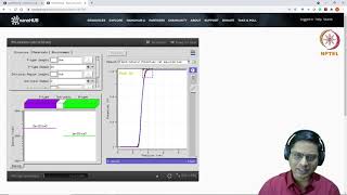
Demo of PN Junction Lab on Nanohub - Lecture 4.6
Explore PN junction behavior using Nanohub's interactive lab simulation. Gain hands-on experience with semiconductor physics concepts.
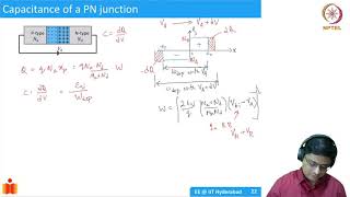
Depletion Capacitance in PN Junction
Explore depletion capacitance in PN junctions, understanding its formation, characteristics, and impact on semiconductor device performance.
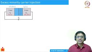
Minority Carrier Injection in PN Junctions - Lecture 5.2
Explore minority carrier injection in PN junctions, examining its principles and effects on semiconductor device behavior.
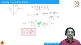
PN Junction Electrostatics: Examples and Analysis - Lecture 4.5
Explore PN junction electrostatics through examples, covering one-sided and linearly graded junctions, built-in potential, and electric field analysis.