Understanding PCB Layout Essentials - Change the Way How You Look at the Tracks
Explore a new perspective on PCB layout, focusing on energy transfer rather than voltages and currents. Learn to optimize designs for improved performance and efficiency.
Generating Manufacturing Outputs for Altium Beginners
Learn to generate essential manufacturing outputs in Altium Designer, including Gerbers, BOMs, assembly drawings, and 3D models. Master the final steps of PCB design for production.
Altium Beginners - Placement, Variants, Assembly Drawings
Learn advanced Altium Designer techniques for PCB layout, including component placement, assembly drawings, and variant creation. Enhance your skills in efficient PCB design workflows.

Altium Beginners - PCB Layout
Step-by-step guide to PCB layout in Altium Designer, covering importing schematics, component placement, layer management, and design rule checks for beginners.
Cadence Allegro Tutorial - How to Create SKILL Script and Your Own Commands
Learn to create and use SKILL scripts for custom commands in Cadence Allegro. Covers script creation, execution, and practical application with downloadable example code.
How to Design Boards That Work the First Time
Learn effective PCB design techniques to create successful first-version boards. Covers schematic design, component selection, layout strategies, and testing considerations for reliable prototypes.
Benefits of Fusion 360 Electronics for Autodesk EAGLE Users - Autodesk Fusion 360
Discover seamless PCB design migration from EAGLE to Fusion 360. Enhance collaboration, improve component placement, and achieve holistic product design with comprehensive electronics and PCB tools.
The Future of Connected PCB
Explore Fusion 360's electronic design features, including schematic simulation, manual routing, PCB outlines, and e-cooling, for comprehensive product design in a single platform.
E-CAD + M-CAD Workflows and Tips
Explore efficient E-CAD and M-CAD workflows using Autodesk Eagle and Fusion 360. Learn time-saving techniques for electronic component cut-outs and PCB design integration.
Routing for High Speed Designs
Analyze high-speed signal routing, learn guidelines, and explore Fusion Electronics tools for efficient PCB design and impedance control.
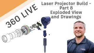
Fusion 360 Live - Laser Projector Project - Creating Exploded View and Drawings
Learn to create exploded views and detailed drawings of a complex laser projector assembly, including techniques for component manipulation, storyboarding, and technical documentation in Fusion 360.
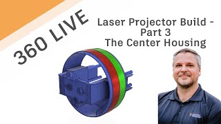
Laser Projector Build - The Center Housing
Detailed walkthrough of creating a laser projector's center housing, covering injection molding, PCB integration, and assembly techniques in Autodesk Fusion 360.
Boggling the Boardhouse - Designing 3D Structures, Circuits, and Sensors from PCBs
Explore innovative PCB design techniques for 3D structures, circuits, and sensors. Learn to overcome common challenges and create unique, functional designs using EAGLE and practical examples.
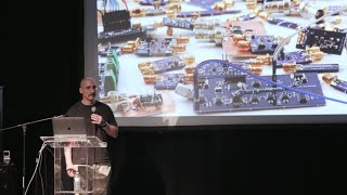
Towards an Open-Source Multi-GHz Sampling Oscilloscope
Explore the challenges and progress in creating an open-source GHz+ sampling oscilloscope, including design insights, technical hurdles, and promising developments in high-frequency measurement technology.

Building Beautiful Boards With Star Simpson
Discover techniques for creating visually stunning PCBs, from variable thickness soldermasks to vector art silkscreens, transforming circuit boards into functional works of art.

Lasers, Projectors, and Custom Hardware for Epic Interactive Experiences
Explore digital art installations combining projectors, lasers, and custom hardware. Learn about interactive experiences and the technology behind magical user interfaces.
Testing Myths of High-Speed PCB Design
Debunking common misconceptions in high-speed PCB design, focusing on EM fields, inductance paths, glass weave effects, and trace angles for improved circuit performance.
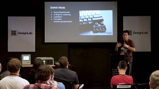
The Engineering and Culture of the Mechanical Keyboard
Explore mechanical keyboard design, technology, and subculture. Learn about custom builds, switch modifications, and PCB design. Discover the engineering behind these specialized input devices.
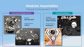
Remoticon 2021 - Debra Ansell Invents Incredibly Clever PCBs
Explore innovative PCB designs for modular LED sculptures and wearables. Learn clever techniques for interconnecting boards, from pressure connectors to rotating joints, pushing the boundaries of electronic creativity.

PCB Reverse Engineering - Eric Schlaepfer
Explore techniques for reverse engineering 2-layer PCBs with Eric Schlaepfer. Learn about tools, components, package types, markings, block diagrams, and circuit analysis in this comprehensive presentation.

Insights on Re-Architecting to a Single Codebase for Multiple Hardware Platforms
Explore strategies for unifying codebases across diverse hardware platforms using Zephyr OS, enhancing efficiency in multi-product portfolios with common sensor and data functionalities.