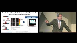
Foundational Tools, Techniques, and Materials for Modern Nanotechnology
Explore foundational tools, techniques, and materials driving the nanotechnology revolution, presented by Chad Mirkin from Northwestern University.
How Sand and Java Are Used to Create the World's Most Powerful Chips
Explore the fascinating world of chip manufacturing, from sand to powerful processors, and discover Java's role in optimizing this cutting-edge process.
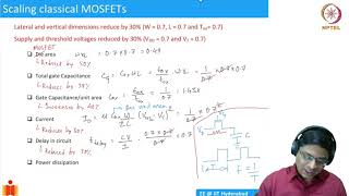
MOSFET Scaling and Technology Nodes - Lecture 10.1
Explore MOSFET scaling principles and technology node advancements in semiconductor manufacturing, enhancing understanding of modern transistor design and fabrication.
Printmaking
Explore five printmaking techniques: relief, intaglio, lithography, silkscreen, and monotype. Learn processes and examine famous works by Rembrandt, Warhol, and others.
Software at ASML: The Force Behind Making Microchips
Explore ASML's software ecosystem driving semiconductor fabrication advancements through innovative development environments and strategic talent initiatives.

Speedrunning 30 Years of Lithography Technology
Explore the journey of replicating 30 years of lithography technology advancements, from assembly challenges to breakthroughs, in this engaging and informative video on semiconductor manufacturing.
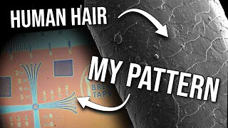
Electron Beam Lithography - Drawing Images with Electrons
Explore electron beam lithography using a scanning electron microscope. Learn about substrates, resists, development, and factors affecting image quality. Discover applications and future possibilities in nanoscale fabrication.
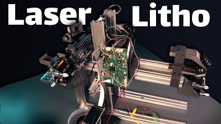
DIY Laser Lithography - Micron Resolution
Explore DIY laser lithography for microfabrication, including techniques, equipment, and results. Learn about maskless photolithography and its applications in creating intricate patterns at micron resolution.
AIM System: Automated Lithography Process Monitoring and Measurement for Semiconductor Manufacturing
Discover how AIM (All wafer Intelligent Monitoring) revolutionizes semiconductor manufacturing by automating lithography process measurements, enhancing yield while maintaining productivity through innovative image-based analysis.
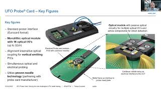
Enabling High Volume Data Communication - Solving Challenges in PIC Wafer Testing
Discover how Photonic Integrated Circuits revolutionize data communication through wafer testing innovations, focusing on Jenoptik's UFO Probe® card for simultaneous electrical and optical testing at high volumes.