Description:
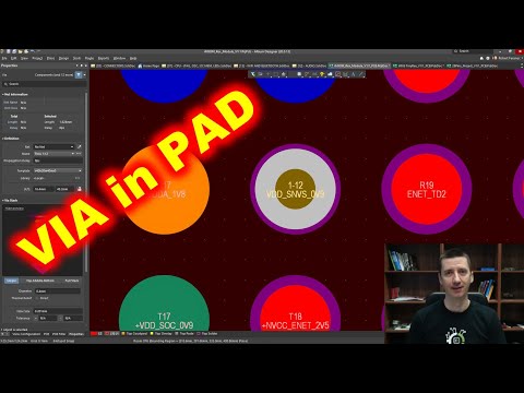
Learn about the critical aspects of using VIA and VIA-in-PAD in PCB design through this comprehensive video tutorial. Explore minimum size requirements, selection criteria, cost considerations, and essential guidelines for implementing VIAs and VIAs in PAD. Discover insights on dimensions, handling, registration, and Laser Direct Imaging techniques. Understand limitations, air trapping issues, and various filling systems including resin and epoxy. Examine potential problems like eyebrow cracks and learn about alternative solutions such as stacked microvias. Gain valuable knowledge on VIA types, plugging methods, and where to send VIAs for manufacturing. Benefit from expert advice provided by Mike from Exception PCB to optimize your PCB design process.
Using VIA in PAD - Guidelines, Dimensions and More
Add to list