Главная
Study mode:
on
1
What you will create
2
Start a new project in EasyEDA
3
Adding USB-C connector to schematic
4
Adding output connector
5
Connecting USB-C
6
Connecting USB-C CC1 and CC2 pins
7
Adding 5.1k resistors
8
Adding 100nF capacitors
9
Adding LED
10
Adding 1k resistor
11
Selecting in EasyEDA
12
Naming nets
13
Creating your own component - Mounting holes
14
Creating footprint in EasyEDA
15
Adding mounting holes to schematic
16
Adding CC pin info into schematic
17
Annotating schematic
18
Enable support for color PCB silkscreen
19
Schematic check - Running ERC
20
Starting PCB
21
Placing big components in PCB MH, J
22
Define board shape
23
Placing small components R, C, D
24
JLCPCB manufacturing capabilities
25
Setting up PCB design rules
26
Hide reference designators
27
Starting PCB Layout
28
Connecting CC pins
29
Connecting GND
30
Draw DIODE connection
31
Making changes in schematic and transferring them to PCB
32
Working with polygons updating, thermal relief
33
Connecting +5V
34
Prohibited region
35
Place reference designators
36
Adding text on silkscreen
37
Adding gold logo
38
Adding color image on silkscreen
39
Starting BOX enclosure
40
Add openings for connectors
41
Add opening for LED
42
Adding support for screws
43
Adding + and - signs
44
Exporting 3D model and 3D printing box
45
Generating manufacturing outputs
46
Generating gerber files for color PCB
47
Replacing color picture with a standard one
48
Generating gerber files for standard PCB
49
Generating BOM Bill of material
50
Generating Pick and Place file
51
Ordering our boards: PCB and Assembly
52
Ordering box
53
Finishing ordering
54
Ordering missing connector
55
Confirming placement and box manufacturing
56
Unpacking our boards
57
Unpacking the 3D printed boxes / enclosures
58
Inspecting the board, soldering down the missing connector
59
Measuring our board
60
Placing board inside of 3D printed box
61
Testing our board
62
Thank you very much for watching
Description:
Save Big on Coursera Plus. 7,000+ courses at $160 off. Limited Time Only! Grab it Learn how to design and manufacture a custom PCB in just two hours with this comprehensive tutorial. Follow along to create a USB-C power supply from scratch using EasyEDA software. Master the process of drawing schematics, PCB layout, and enclosure design. Gain hands-on experience with component selection, footprint creation, and board shape definition. Explore advanced techniques like adding color silkscreen images and generating manufacturing outputs. Discover the intricacies of ordering PCBs, components, and 3D-printed enclosures. By the end of this tutorial, you'll have the skills to design, manufacture, and assemble your own custom PCB projects.

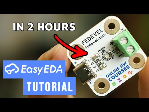
Custom PCB Design Tutorial - From Schematic to Manufacturing in EasyEDA

Robert Feranec
Add to list