Description:
Learn how to create perfect PCB footprints in this comprehensive 2-hour and 18-minute video tutorial. Explore essential topics such as optimal pad dimensions, proper pin 1 placement, the importance of following standards, and the role of IPC in PCB design. Gain insights from industry expert Tom Hausherr and discover valuable resources like PCB Libraries. Delve into crucial aspects of PCB design, including toe and heel considerations, soldering standards, IPC 7351 and 735 guidelines, PCB path size software, density levels, and troubleshooting issues like excessive solder. Examine various component types, including Goldwing lead, dual flat no-lead parts, and thermal pads. Master the art of creating precise PCB footprints to enhance your electronic design skills and produce high-quality circuit boards.
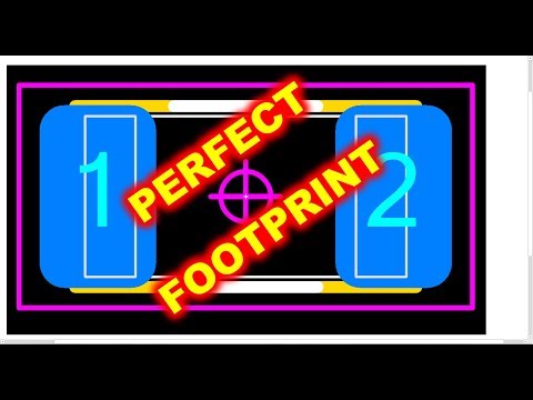
How to Create Perfect PCB Footprint - What You Really Need to Know
Add to list