Description:
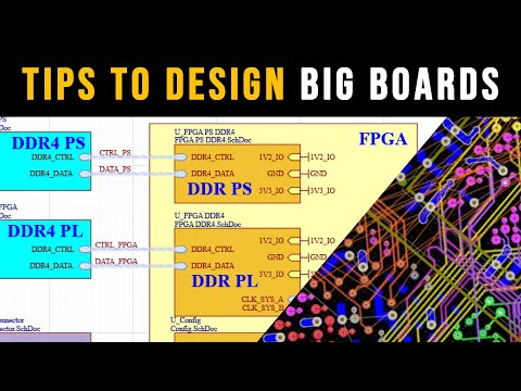
Discover valuable insights and techniques for designing complex boards, particularly those involving large FPGAs, in this comprehensive video tutorial. Learn about schematic symbols, pin management, hierarchical design, and power optimization from industry expert Marko Hoepken. Explore topics such as footprint creation, fanout strategies for large FPGA packages, layout considerations, and length matching. Gain practical advice on building prototypes and reducing complexity in board design. Master the art of designing intricate boards with these expert tips and tricks, applicable to FPGA and other complex electronic designs.
How Are Big FPGA and Other Boards Designed - Tips and Tricks
Add to list
#Engineering
#Electrical Engineering
#Circuits
#FPGA
#Art & Design
#Design & Creativity
#Prototyping