Description:
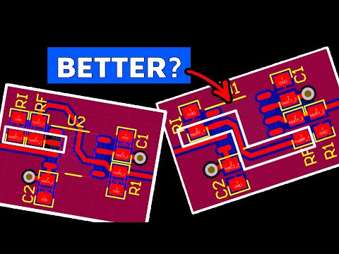
Discover essential tips for designing boards with analog, digital, and operational amplifiers in this comprehensive video lecture. Learn about floor planning and component placement, managing return current, mitigating crosstalk, handling split planes and ground considerations, and optimizing op amp layouts. Explore decoupling techniques, electrical overstress protection, and the importance of component specifications. Gain insights into common mode noise rejection, power supply noise rejection, and the role of simulations in design. Understand the limitations of measurements, proper oscilloscope usage, and the significance of board cleanliness. Delve into practical examples demonstrating common mode and power supply noise rejection, and learn when to consider fixing a working design. Utilize evaluation modules to enhance your design process and improve overall board performance.
10 Tips for Analog, Mixed-Signal, and Op Amp Circuit Design
Add to list
#Engineering
#Electronics
#Operational Amplifiers
#Electrical Engineering
#Digital Signal Processing
#Audio Processing
#Noise Reduction
#PCB Layout
#Signal Integrity