Главная
Study mode:
on
1
https://courses.fedevel.com/itemDetail.html?itemtype=course&dbid=1569758378867&instrid=us-east-2_KpwYC7yKf6c01d-ccc8-43e0-8f33-c5a70caf707f
2
Introduction
3
What you will learn
4
*** Starting a new project ***
5
Creating a component in OrCAD - Header
6
Drawing a schematic symbol in OrCAD
7
Adding Part number property to symbol
8
Creating resistor schematic symbol
9
Creating LED schematic symbol
10
*** Drawing schematic in OrCAD ***
11
Creating a through hole pad in Padstack Editor
12
Creating SMD pad for resistor
13
Creating SMD pad for LED
14
Creating a VIA in Padstack Editor
15
*** Creating footprints in Allegro ***
16
Creating footprint for header
17
Adding 3D model to footprint in Allegro
18
Creating LED footprint
19
Creating Resistor footprint in Allegro
20
Adding footprint to schematic symbol
21
Correcting symbol and updating schematic
22
Annotating schematic in OrCAD
23
How to fix missing footprint warning in OrCAD
24
Running DRC Design Rules Check in OrCAD
25
*** Starting PCB in Allegro ***
26
Changing board shape
27
Placing components into PCB in Allegro
28
Setting up rules in Allegro
29
Setting up PCB stackup in Allegro
30
Routing PCB in Allegro
31
Editing Schematic and importing the changes into existing PCB
32
Editing footprint and importing changes into existing PCB
33
Improving Silkscreen layer - Moving and Adding Text
34
3D model of our PCB
35
Creating Views
36
Checking and fixing errors on PCB in Allegro
37
*** Generating outputs for manufacturing ***
38
Generating Gerber files
39
Generating NC Drill file
40
Printing Assembly Drawing layers into PDF
41
Printing any combination of layers in Allegro
42
Generating Pick and Place file
43
Printing Schematic in OrCAD
44
Generating BOM Bill of Material
45
Download finished project
46
Online courses to learn about electronics
Description:
Learn to design PCBs using Cadence OrCAD and Allegro 17.4 in this comprehensive tutorial for beginners. Start from scratch and progress through creating components, drawing schematics, designing footprints, and routing PCBs. Master essential skills like setting up design rules, editing existing designs, and generating manufacturing outputs including Gerber files, assembly drawings, and bills of materials. Follow along with step-by-step instructions covering the entire PCB design workflow, from initial project setup to final production files. Gain hands-on experience with industry-standard EDA tools and techniques used by professional PCB designers.

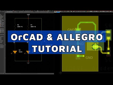
OrCAD and Cadence Allegro PCB Editor - Step by Step for Beginners

Robert Feranec
Add to list